


The Curse of Moore’s Law — The Truth Behind the 2nm Process
A symbolic number — and an architectural truth.

Did you know that in a “2nm process” chip, not a single wire is actually 2 nanometers wide?
In fact, the term “2nm process” doesn’t refer to the physical dimensions of a transistor. It’s a marketing term used to denote a “generation” of semiconductor technology.
While this is common knowledge within the semiconductor industry, I only realized it recently, despite working in the field for years.
Historically, terms like “x nm” referred to the smallest features on a chip, so I naturally assumed that 2nm meant there were 2nm-width lines somewhere in the layout.
My background was in what’s now called “legacy” processes, not cutting-edge, so I didn’t question it.
Even in those legacy nodes, we were always pushing the physical limits of miniaturization. So when I heard “2nm,” I just thought, “Wow, the frontline engineers must really be working hard.”
But if 2nm isn’t a real measurement, what is it based on?
There’s a predictive rule in semiconductors known as Moore’s Law: the number of transistors on a chip doubles every two years.
To stay on that log-linear trend, the industry relentlessly pursued miniaturization — shrinking every possible feature to cram more transistors into the same area.
The key to miniaturization is lithography wavelength. Shorter wavelengths allow for smaller features.
From g-line (436nm) to i-line (365nm), KrF (248nm), ArF (193nm), and finally EUV (13.5nm), the litho roadmap kept evolving — until it basically hit a wall.
With ArF, you could push it down to ~20nm using optical tricks, material tunings and process optimizations. But EUV? Not so much.
According to ASML, the sole EUV equipment provider, the resolution limit for EUV with NA 0.33 is 13nm.
So realistically, the smallest manufacturable dimensions hover around that mark.
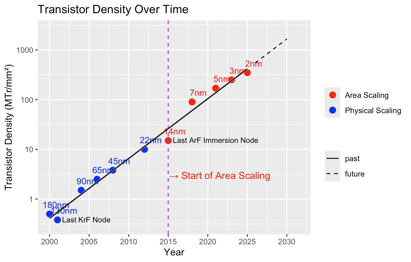
By the 2010s, physical miniaturization was approaching its limit. Moore’s Law seemed doomed — until a shift in transistor architecture saved it.
Enter: FinFET
With its 3D structure, FinFET allowed for higher transistor density without reducing wire widths. This is when the industry transitioned to a new definition for process nodes: Area scaling, not physical scaling.
In 2015, the “14nm” FinFET node debuted. This was the first process named under the area-scaling regime.
Back then, only Intel, TSMC, and Samsung used FinFET, and they didn’t really talk about the disconnect between node names and physical dimensions.
In 2019, Intel began volume production with its 10nm node — functionally equivalent to TSMC’s 7nm.
By 2021, TSMC launched 5nm; then 3nm in 2023; and 2nm in 2025.
Since 2015, all node names have represented transistor density improvements, not physical line widths.
That’s how the industry has kept Moore’s Law alive — not through literal size reductions, but through clever 3D design and density metrics.
GAA — Gate-All-Around
Now, let’s talk about GAA.
After 5nm and 3nm, FinFET hit its limits. You could only raise those “fins” so high, and shrink them so much. GAA surrounds the channel with the gate on all sides, boosting electrostatic control and enabling even greater scaling.
Today’s “2nm process” marks the debut of GAA. It’s not about shrinking wires further — it’s the culmination of architectural evolution.
And so, the industry keeps marching forward under the name “2nm,” even if no feature measures 2 nanometers.
(Transistor densities were estimated from public data such as transistor counts and die areas listed on Wikipedia – Transistor Count.)
Why?
Because clinging to Moore’s Law has driven the innovation that got us here.
Even if it’s no longer about size, the name represents the marketing pressure and investor dreams that keep engineers working weekends to keep Moore’s Law still alive.
Yes, today’s transistor densities may look inflated by naming conventions — but behind the names, and especially with the shift to 3D architectures, the progress is real. And it’s been hard-won. Not through shrinking dimensions — but through rethinking what scaling truly means.
Thanks for reading!
References:
Historical transistor counts and die sizes referenced from Wikipedia – Transistor Count.